Table of Contents
Overview
Multi-channel PWM signal generation with a dsPIC33 microcontroller involves generating multiple PWM signals simultaneously on different output pins. This capability allows you to control multiple actuators, such as motors or LEDs, with individual PWM signals.
Required components
| S.No | COMPONENTS | QUANTITY | |
| 1 | DSPIC33FJ64GS606 | 1 | Amazon |
| 2 | PICkit4 Programmer | 1 | Amazon |
| 3 | Oscilloscope | 1 | Amazon |
| 4 | Logic Analyser | 1 | Amazon |
| 5 | connection wires | 1 | Amazon |
Here’s an overview of the steps involved in generating multi-channel PWM signals with a dsPIC33 microcontroller:
Introduction about PWM
PWM (Pulse Width Modulation) is a widely used technique in embedded systems to control the average power or intensity of a signal by varying its duty cycle. It involves toggling a signal between high and low states at a fixed frequency while adjusting the duration of the high state (duty cycle). By changing the duty cycle, the average power or intensity of the signal can be controlled.
The dsPIC33 microcontroller provides dedicated hardware modules specifically designed for PWM signal generation. These modules have registers and features that allow you to configure and control multiple PWM channels simultaneously. The number of available PWM channels depends on the specific dsPIC33 model.
To generate multi-channel PWM signals with a dsPIC33 microcontroller, you typically follow these steps:
Configure the PWM Module
Initialize the PWM module by setting the necessary registers. This includes configuring the PWM time base, period, and other parameters specific to the dsPIC33 microcontroller model you are using.
Assign Output Pins
Select the output pins that will generate the PWM signals. The dsPIC33 microcontroller provides several pins with PWM functionality. You need to assign these pins to the desired PWM channels.
Set PWM Parameters
Set the parameters for each PWM channel, such as the period and duty cycle. The specific register settings will depend on your dsPIC33 microcontroller model. Refer to the datasheet and reference manual for the correct register names and values.
Enable PWM Output
Enable the PWM output for the selected pins. This step allows the PWM signals to be generated on the assigned output pins.
Update Duty Cycles
Continuously update the duty cycle values for each PWM channel as needed. You can do this within a loop or using interrupts, depending on your application requirements. Changing the duty cycle allows you to control the average power or intensity of each PWM signal.
Control Multiple Channels
With the multi-channel PWM capability, you can independently control multiple PWM signals by adjusting their duty cycles. This allows you to create complex control schemes for various actuators in your system.
Register settings
To generate a PWM signal with a dsPIC33 microcontroller, you will typically use the following registers:
- PTCON (PWM Time Base Control Register)
- PTPER (PWM Time Base Period Register)
- PWMxCON1 (PWM Control Register 1)
- PWMxCON2 (PWM Control Register 2)
- PDCx (PWM Duty Cycle Register)
- SEVTCMPx (Special Event Compare Register)
- PTPER – Setting the Period Value
Let’s explore some specific register settings and their functions:
PTCONbits.PTEN
The line PTCONbits.PTEN = 0; is used to disable the PWM module in a dsPIC33 microcontroller. Here’s what it does:
The PTCON register is a control register that is used to enable or disable the PWM module and configure various PWM module options. The PTCONbits.PTEN bit is a specific bit within the PTCON register that controls the overall enable/disable state of the PWM module.
Setting PTCONbits.PTEN = 0; clears the PTEN bit, which disables the PWM module. When the PWM module is disabled, it stops generating PWM signals on the configured output pins. This can be useful when you want to pause or stop the generation of PWM signals temporarily.
To enable the PWM module again and resume generating PWM signals, you can set PTCONbits.PTEN= 1;, which sets the PTEN bit and enables the PWM module.
TRISEbits.TRISE0
The line TRISEbits.TRISE0 = 0; is used to configure the data direction of a specific pin in the Port E (RE0) as an output in a dsPIC33 microcontroller. Let’s break down the usage:
TRISE is the register that controls the data direction of the Port E pins. TRISEbits refers to the individual bits within the TRISE register. TRISE0 corresponds to the specific bit that controls the data direction of pin RE0 in Port E.
By setting TRISEbits.TRISE0 = 0;, you are configuring pin RE0 as an output. This means that you can use this pin to drive a signal or control an external device connected to it.
On the other hand, if you want to configure pin RE0 as an input, you would set TRISEbits.TRISE0 = 1;.
IOCON1bits.PENH and IOCON1bits.PENL
The lines IOCON1bits.PENH = 1; and IOCON1bits.PENL = 0; are used to enable the PWM output on the high side and disable the PWM output on the low side of PWM channel 1 in a dsPIC33 microcontroller. Let’s break down the usage:
IOCON1 is the register that controls the PWM Output Control 1 configuration for a specific PWM channel. IOCON1bits refers to the individual bits within the IOCON1 register. PENH is the specific bit that enables or disables the PWM output on the high side of PWM channel 1. PENL is the specific bit that enables or disables the PWM output on the low side of PWM channel 1.
By setting IOCON1bits.PENH = 1;, you are enabling the PWM output on the high side of PWM channel 1. This means that the PWM signal will be generated on the configured output pin for the high side of the PWM channel.
By setting IOCON1bits.PENL = 0;, you are disabling the PWM output on the low side of PWM channel 1. This means that the PWM signal will not be generated on the configured output pin for the low side of the PWM channel.
To enable the PWM output on the low side of PWM channel 1, you would set IOCON1bits.PENL = 1;. In this case, the PWM signal would be generated on the configured output pin for the PTPER – Setting the Period
PTPER – Setting the Period Value
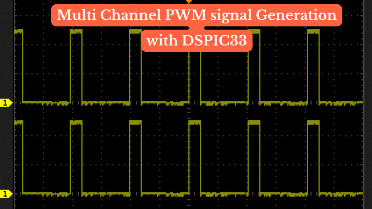
The PTPER register is responsible for setting the period value for the PWM time base. In this case, a period value of 20000 has been specified. This means that each PWM cycle will have a total time duration of 20000 units. Simply put, it determines the time it takes for the PWM signal to complete one full cycle.
PDC1 – Duty Cycle for PWM Channel 1
Moving on to the first PWM channel, PDC1 comes into play. This register allows you to set the duty cycle for PWM channel 1. In the provided example, a duty cycle of 10047 has been set. The duty cycle represents the “ON” time of the PWM signal relative to the period. In other words, for channel 1, the PWM signal will be “ON” for 10047 units of the total 20000 unit period.
PDC2 – Duty Cycle for PWM Channel 2
Now let’s shift our focus to PWM channel 2. The duty cycle for this channel is controlled by the PDC2 register. According to the values you’ve given, a duty cycle of 6666 has been assigned. This means that for channel 2, the PWM signal will be “ON” for 6666 units of the total 20000 unit period.
PDC3 – Duty Cycle for PWM Channel 3
Similarly, PDC3 takes charge of setting the duty cycle for PWM channel 3. With a specified duty cycle of 5000, this channel’s PWM signal will be “ON” for 5000 units of the total 20000 unit period.
PDC4 – Duty Cycle for PWM Channel 4
Last but not least, we have PDC4, which is responsible for determining the duty cycle for PWM channel 4. As per the given values, a duty cycle of 10047 has been set for this channel. Thus, during each cycle, the PWM signal for channel 4 will exhibit an “ON” time of 10047 units out of the total 20000 unit period.
/*
 * File:   main.c
 * Author: Admin
 *
 */

#include "xc.h"
#include <p33FJ64GS606.h>
#include "stdio.h"
#include "stdlib.h"
#include <string.h>
#include <math.h>
#include <dsp.h>

// DSPIC33FJ64GS606 Configuration Bit Settings

// 'C' source line config statements

// FBS
#pragma config BWRP = WRPROTECT_OFF     // Boot Segment Write Protect (Boot Segment may be written)
#pragma config BSS = NO_FLASH           // Boot Segment Program Flash Code Protection (No Boot program Flash segment)

// FGS
#pragma config GWRP = OFF               // General Code Segment Write Protect (General Segment may be written)
#pragma config GSS = OFF                // General Segment Code Protection (General Segment Code protect is disabled)

// FOSCSEL
#pragma config FNOSC = FRCDIVN          // Oscillator Source Selection (Internal Fast RC (FRC) Oscillator with postscaler)
#pragma config IESO = ON                // Internal External Switch Over Mode (Start up device with FRC, then switch to user-selected oscillator source)

// FOSC
#pragma config POSCMD = NONE            // Primary Oscillator Source (Primary Oscillator disabled)
#pragma config OSCIOFNC = OFF           // OSC2 Pin Function (OSC2 is clock output)
#pragma config FCKSM = CSDCMD           // Clock Switching Mode bits (Both Clock switching and Fail-safe Clock Monitor are disabled)

// FWDT
#pragma config WDTPOST = PS32768        // Watchdog Timer Postscaler (1:32,768)
#pragma config WDTPRE = PR128           // WDT Prescaler (1:128)
#pragma config WINDIS = OFF             // Watchdog Timer Window (Watchdog Timer in Non-Window mode)
#pragma config FWDTEN = OFF             // Watchdog Timer Enable (Watchdog timer enabled/disabled by user software)

// FPOR
#pragma config FPWRT = PWR128           // POR Timer Value (128ms)
#pragma config ALTSS1 = ON              // Enable Alternate SS1 pin bit (SS1A is selected as the I/O pin for SPI1)
#pragma config ALTQIO = OFF             // Enable Alternate QEI1 pin bit (QEA1, QEB1, INDX1 are selected as inputs to QEI1)

// FICD
#pragma config ICS = PGD1               // Comm Channel Select (Communicate on PGC1/EMUC1 and PGD1/EMUD1)
#pragma config JTAGEN = OFF             // JTAG Port Enable (JTAG is disabled)

// FCMP
#pragma config HYST0 = HYST45           // Even Comparator Hysteresis Select (45 mV Hysteresis)
#pragma config CMPPOL0 = POL_FALL       // Comparator Hysteresis Polarity (for even numbered comparators) (Hysteresis is applied to falling edge)
#pragma config HYST1 = HYST45           // Odd Comparator Hysteresis Select (45 mV Hysteresis)
#pragma config CMPPOL1 = POL_FALL       // Comparator Hysteresis Polarity (for odd numbered comparators) (Hysteresis is applied to falling edge)

// #pragma config statements should precede project file includes.
// Use project enums instead of #define for ON and OFF.


// ------------------- PWM  ---------------------------- //

#define PWM1L					LATEbits.LATE0		// PWM 1 low switch I/O pin
#define PWM2L					LATEbits.LATE2		// PWM 2 low switch I/O pin
#define PWM3L					LATEbits.LATE4		// PWM 3 low switch I/O pin
#define PWM4L					LATEbits.LATE6		// PWM 4 low switch I/O pin

void initPWM(void);
int main(void) {

PTCONbits.PTEN = 0;      						/* Enable the PWM Module */
//------------------- Start ------------------------//

	// PWM  GPIO
    TRISEbits.TRISE0    = 0;							// PWM 1L
    TRISEbits.TRISE2    = 0;							// PWM 2L
	TRISEbits.TRISE4    = 0;							// PWM 3L
    TRISEbits.TRISE6    = 0;							// PWM 4L
    initPWM();
    while(1)
    {

    }

}

void initPWM(void)
{
    PTCONbits.PTEN = 0;      			  /* Enable the PWM Module */
	PTCON2bits.PCLKDIV = 2;
    PTPER = 20000; // Time periode

    /*~~~~~~~~~~~~~~~~~~~~~~~ PWM1 Configuration ~~~~~~~~~~~~~~~~~~~~~~~~~~~~*/
    IOCON1bits.PENH 	 = 1;      			/* PWM1H is controlled by pwm module */
    IOCON1bits.PENL 	 = 0;      			/* PWM1L is controlled by GPIO module */
	IOCON1bits.POLH		 = 0;               /* Drive signals are active-high */
	IOCON1bits.POLL		 = 0;               /* Drive signals are active-high */
    IOCON1bits.PMOD 	 = 0;      			/* Select Complementary PWM Output mode */
    IOCON1bits.OVRENH	 = 0;				/* Disable Override feature for shutdown PWM */
    IOCON1bits.OVRENL	 = 0;				/* Disable Override feature for shutdown PWM */
    IOCON1bits.OVRDAT	 = 0;			    /* Shut down PWM with Over ride 0 on PWMH and PWML */
    IOCON1bits.SWAP		 = 0;               /* Swap Drive signals  */


	/*~~~~~~~~~~~~~~~~~~~~~~~ PWM2 Configuration ~~~~~~~~~~~~~~~~~~~~~~~~~~~~*/
    IOCON2bits.PENH 	 = 1;      			/* PWM2H is controlled by pwm module */
    IOCON2bits.PENL 	 = 0;      			/* PWM2L is controlled by GPIO module */
	IOCON2bits.POLH		 = 0;               /* Drive signals are active-high */
	IOCON2bits.POLL		 = 0;               /* Drive signals are active-high */
    IOCON2bits.PMOD 	 = 0;      			/* Select Complementary PWM Output mode */
    IOCON2bits.OVRENH	 = 0;				/* Disable Override feature for shutdown PWM */
    IOCON2bits.OVRENL	 = 0;				/* Disable Override feature for shutdown PWM */
    IOCON2bits.OVRDAT	 = 0;			    /* Shut down PWM with Over ride 0 on PWMH and PWML */
    IOCON2bits.SWAP		 = 0;               /* Swap Drive signals  */

    /*~~~~~~~~~~~~~~~~~~~~~~~ PWM3 Configuration ~~~~~~~~~~~~~~~~~~~~~~~~~~~~*/
    IOCON3bits.PENH 	 = 1;      			/* PWM3H is controlled by pwm module */
    IOCON3bits.PENL 	 = 0;      			/* PWM3L is controlled by GPIO module */
	IOCON3bits.POLH		 = 0;               /* Drive signals are active-high */
	IOCON3bits.POLL		 = 0;               /* Drive signals are active-high */
    IOCON3bits.PMOD 	 = 0;      			/* Select Complementary PWM Output mode */
    IOCON3bits.OVRENH	 = 0;				/* Disable Override feature for shutdown PWM */
    IOCON3bits.OVRENL	 = 0;				/* Disable Override feature for shutdown PWM */
    IOCON3bits.OVRDAT	 = 0;			    /* Shut down PWM with Over ride 0 on PWMH and PWML */
    IOCON3bits.SWAP		 = 0;               /* Swap Drive signals  */

    /*~~~~~~~~~~~~~~~~~~~~~~~ PWM4 Configuration ~~~~~~~~~~~~~~~~~~~~~~~~~~~~*/
    IOCON4bits.PENH 	 = 1;      			/* PWM3H is controlled by pwm module */
    IOCON4bits.PENL 	 = 0;      			/* PWM3L is controlled by GPIO module */
	IOCON4bits.POLH		 = 0;               /* Drive signals are active-high */
	IOCON4bits.POLL		 = 0;               /* Drive signals are active-high */
    IOCON4bits.PMOD 	 = 0;      			/* Select Complementary PWM Output mode */
    IOCON4bits.OVRENH	 = 0;				/* Disable Override feature for shutdown PWM */
    IOCON4bits.OVRENL	 = 0;				/* Disable Override feature for shutdown PWM */
    IOCON4bits.OVRDAT	 = 0;			    /* Shut down PWM with Over ride 0 on PWMH and PWML */
    IOCON4bits.SWAP		 = 0;               /* Swap Drive signals  */


    PDC1 = 10047;                           /* 50% (0) Initial Duty cycle */
    PDC2 = 6666;                            /* 75% (0) Initial Duty cycle */
	PDC3 = 5000; 							/* 25% (0) Initial Duty cycle */
    PDC4 = 10047; 							/* 50% (0) Initial Duty cycle */

    IFS5bits.PWM1IF		 = 0;    			// Clear PWM1 interrupt flag
	IFS5bits.PWM2IF		 = 0;    			// Clear PWM2 interrupt flag
	IFS6bits.PWM3IF		 = 0;    			// Clear PWM3 interrupt flag
    IFS6bits.PWM4IF		 = 0;    			// Clear PWM3 interrupt flag

	PWMCON1bits.TRGIEN	 = 1;    	 		/* trigger event generates an interrupt request */
    PTCONbits.PTEN		 = 1;      			/* Enable the PWM Module */

}