
MICROCONTROLLER
Microprocessors and microcontrollers are widely used in embedded systems products. Microcontroller is a programmable device. A microcontroller has a CPU in addition to a fixed amount of RAM, ROM, I/O ports and a timer embedded all on a single chip. The fixed amount of on-chip ROM, RAM and number of I/O ports in microcontrollers makes them ideal for many applications in which cost and space are critical.
The Intel 8052 is Harvard architecture, single chip microcontroller (µC) which was developed by Intel in 1980 for use in embedded systems. It was popular in the 1980s and early 1990s, but today it has largely been superseded by a vast range of enhanced devices with 8052-compatible processor cores that are manufactured by more than 20 independent manufacturers including Atmel, Infineon Technologies and Maxim Integrated Products.
8052 is an 8-bit processor, meaning that the CPU can work on only 8 bits of data at a time. Data larger than 8 bits has to be broken into 8-bit pieces to be processed by the CPU. 8052 is available in different memory types such as UV-EPROM, Flash and NV-RAM.
The present project is implemented on Keil uVision. In order to program the device, proload tool has been used to burn the program onto the microcontroller.
The features, pin description of the microcontroller and the software tools used are discussed in the following sections.
FEATURES
• Compatible with MCS-51® Products
• 8K Bytes of In-System Programmable (ISP) Flash Memory
– Endurance: 1000 Write/Erase Cycles
• 4.0V to 5.5V Operating Range
• Fully Static Operation: 0 Hz to 33 MHz
• Three-level Program Memory Lock
• 256 x 8-bit Internal RAM
• 32 Programmable I/O Lines
• Three 16-bit Timer/Counters
• Eight Interrupt Sources
• Full Duplex UART Serial Channel
• Low-power Idle and Power-down Modes
• Interrupt Recovery from Power-down Mode
• Watchdog Timer
• Dual Data Pointer
• Power-off Flag
DESCRIPTION
The AT89S52 is a low-power, high-performance CMOS 8-bit microcontroller with 8K bytes of in-system programmable Flash memory. The device is manufactured using Atmel’s high-density nonvolatile memory technology and is compatible with the industry- standard 80C51 instruction set and pinout. The on-chip Flash allows the program memory to be reprogrammed in-system or by a conventional nonvolatile memory programmer. By combining a versatile 8-bit CPU with in-system programmable Flash on a monolithic chip, the Atmel AT89S52 is a powerful microcontroller which provides a highly-flexible and cost-effective solution to many embedded control applications.
The AT89S52 provides the following standard features: 8K bytes of Flash, 256 bytes of RAM, 32 I/O lines, Watchdog timer, two data pointers, three 16-bit timer/counters, a six-vector two-level interrupt architecture, a full duplex serial port, on-chip oscillator, and clock circuitry. In addition, the AT89S52 is designed with static logic for operation down to zero frequency and supports two software selectable power saving modes.
The Idle Mode stops the CPU while allowing the RAM, timer/counters, serial port, and interrupt system to continue functioning. The Power-down mode saves the RAM contents but freezes the oscillator, disabling all other chip functions until the next interrupt or hardware reset.
PIN CONFIGURATIONS

PIN DESCRIPTION
VCC
Supply voltage.
GND
Ground.
Port 0
Port 0 is an 8-bit open drain bidirectional I/O port. As an output port, each pin can sink eight TTL inputs. When 1s are written to port 0 pins, the pins can be used as high impedance inputs. Port 0 can also be configured to be the multiplexed low order address/data bus during accesses to external program and data memory. In this mode, P0 has internal pullups. Port 0 also receives the code bytes during Flash programming and outputs the code bytes during program verification. External pullups are required during program verification.
Port 1
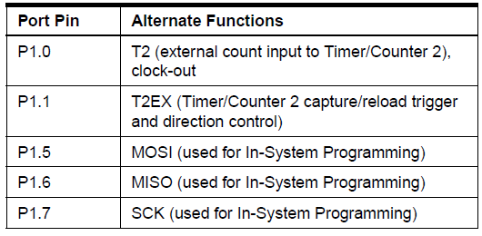
Port 1 is an 8-bit bidirectional I/O port with internal pullups. The Port 1 output buffers can sink/source four TTL inputs. When 1s are written to Port 1 pins, they are pulled high by the internal pullups and can be used as inputs. As inputs, Port 1 pins that are externally being pulled low will source current (IIL) because of the internal pullups. In addition, P1.0 and P1.1 can be configured to be the timer/counter 2 external count input (P1.0/T2) and the timer/counter 2 trigger input (P1.1/T2EX), respectively, as shown in the following table. Port 1 also receives the low-order address bytes during Flash programming and verification.
Port 2
Port 2 is an 8-bit bidirectional I/O port with internal pullups. The Port 2 output buffers can sink/source four TTL inputs. When 1s are written to Port 2 pins, they are pulled high by the internal pullups and can be used as inputs. As inputs, Port 2 pins that are externally being pulled low will source current (IIL) because of the internal pullups. Port 2 emits the high-order address byte during fetches from external program memory and during accesses to external data memory that use 16-bit addresses (MOVX @ DPTR). In this application, Port 2 uses strong internal pull-ups when emitting 1s. During accesses to external data memory that use 8-bit addresses (MOVX @ RI), Port 2 emits the contents of the P2 Special Function Register. Port 2 also receives the high-order address bits and some control signals during Flash programming and verification.
Port 3
Port 3 is an 8-bit bidirectional I/O port with internal pullups. The Port 3 output buffers can sink/source four TTL inputs. When 1s are written to Port 3 pins, they are pulled high by the internal pullups and can be used as inputs. As inputs, Port 3 pins that are externally being pulled low will source current (IIL) because of the pullups. Port 3 also serves the functions of various special features of the AT89S52, as shown in the following table. Port 3 also receives some control signals for Flash programming and verification.

RST
Reset input. A high on this pin for two machine cycles while the oscillator is running resets the device. This pin drives High for 96 oscillator periods after the Watchdog times out. The DISRTO bit in SFR AUXR (address 8EH) can be used to disable this feature. In the default state of bit DISRTO, the RESET HIGH out feature is enabled.
ALE/PROG
Address Latch Enable (ALE) is an output pulse for latching the low byte of the address during accesses to external memory. This pin is also the program pulse input (PROG) during Flash programming. In normal operation, ALE is emitted at a constant rate of 1/6 the oscillator frequency and may be used for external timing or clocking purposes. Note, however, that one ALE pulse is skipped during each access to external data memory. If desired, ALE operation can be disabled by setting bit 0 of SFR location 8EH. With the bit set, ALE is active only during a MOVX or MOVC instruction. Otherwise, the pin is weakly pulled high. Setting the ALE-disable bit has no effect if the microcontroller is in external execution mode.
PSEN
Program Store Enable (PSEN) is the read strobe to external program memory. When the AT89S52 is executing code from external program memory, PSEN is activated twice each machine cycle, except that two PSEN activations are skipped during each access to external data memory.
EA/VPP
External Access Enable. EA must be strapped to GND in order to enable the device to fetch code from external program memory locations starting at 0000H up to FFFFH. Note, however, that if lock bit 1 is programmed, EA will be internally latched on reset.
EA should be strapped to VCC for internal program executions. This pin also receives the 12-volt programming enable voltage (VPP) during Flash programming.
XTAL1
Input to the inverting oscillator amplifier and input to the internal clock operating circuit.
XTAL2
Output from the inverting oscillator amplifier.
XTAL1 and XTAL2 are the input and output, respectively, of an inverting amplifier that can be configured for use as an on-chip oscillator, as shown in Figure. Either a quartz crystal or ceramic resonator may be used. To drive the device from an external clock source, XTAL2 should be left unconnected while XTAL1 is driven, as shown in the below figure. There are no requirements on the duty cycle of the external clock signal, since the input to the internal clocking circuitry is through a divide-by-two flip-flop, but minimum and maximum voltage high and low time specifications must be observed.
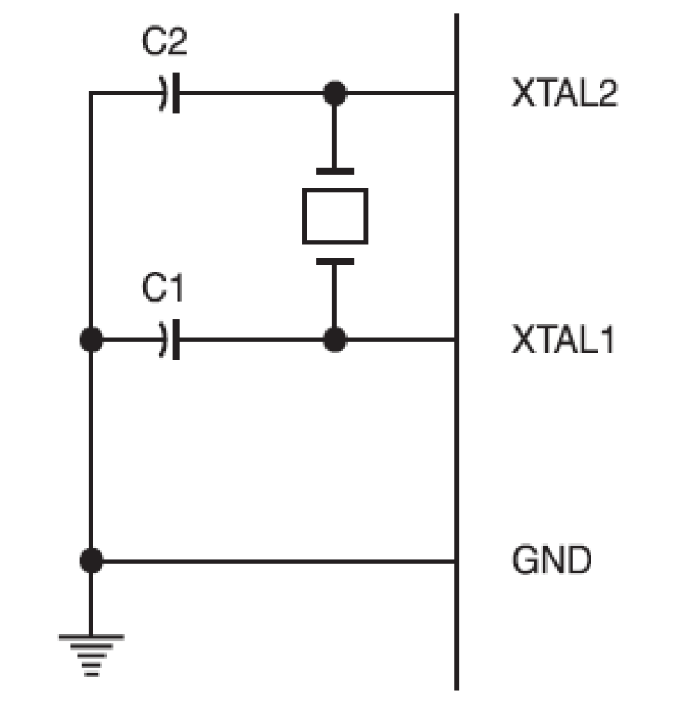
C1, C2 = 30 pF ± 10 pF for Crystals
= 40 pF ± 10 pF for Ceramic Resonators

8052 MICROCONTROLLER MEMORY ORGANIZATION
The microcontroller memory is divided into Program Memory and Data Memory. Program Memory (ROM) is used for permanent saving program being executed, while Data Memory (RAM) is used for temporarily storing and keeping intermediate results and variables. Depending on the model in use (still referring to the whole 8052 microcontroller family) at most a few Kb of ROM and 128 or 256 bytes of RAM can be used. However…
All 8052 microcontrollers have 16-bit addressing bus and can address 64 kb memory. It is neither a mistake nor a big ambition of engineers who were working on basic core development. It is a matter of very clever memory organization which makes these controllers a real “programmers’ tidbit“.
Program Memory
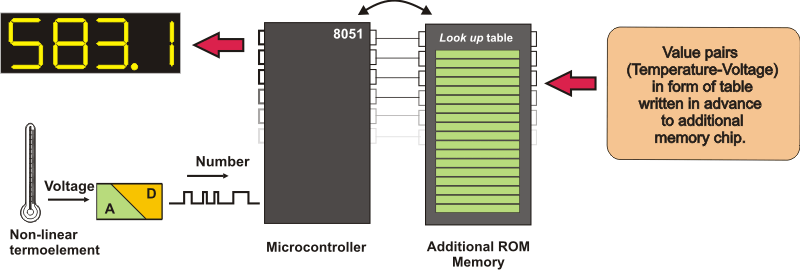
The oldest models of the 8052 microcontroller family did not have any internal program memory. It was added from outside as a separate chip. These models are recognizable by their label beginning with 803 (for ex. 8031 or 8032). All later models have a few Kbytes ROM embedded, Even though it is enough for writing most of the programs, there are situations when additional memory is necessary. A typical example of it is the use of so called lookup tables. They are used in cases when something is too complicated or when there is no time for solving equations describing some process. The example of it can be totally exotic (an estimate of self-guided rockets’ meeting point) or totally common (measuring of temperature using non-linear thermo element or asynchronous motor speed control). In those cases all needed estimates and approximates are executed in advance and the final results are put in the tables (similar to logarithmic tables).
How does the microcontroller handle external memory depend on the pin EA logic state?

EA=0
In this case, internal program memory is completely ignored, only a program stored in external memory is to be executed.
EA=1
In this case, a program from built-in ROM is to be executed first (to the last location). Afterwards, the execution is continued by reading additional memory.
in both cases, P0 and P2 are not available to the user because they are used for data and address transmission. Besides, the pins ALE and PSEN are used too.
Data Memory
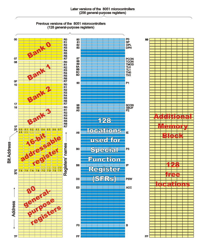
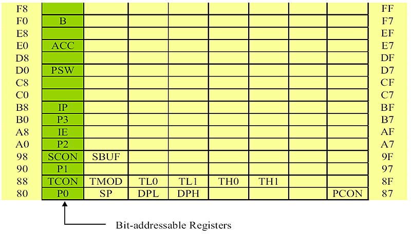
As already mentioned, Data Memory is used for temporarily storing and keeping data and intermediate results created and used during microcontroller’s operating. Besides, this microcontroller family includes many other registers such as: hardware counters and timers, input/output ports, serial data buffers etc. The previous versions have the total memory size of 256 locations, while for later models this number is incremented by additional 128 available registers. In both cases, these first 256 memory locations (addresses 0-FFh) are the base of the memory. Common to all types of the 8052 microcontrollers. Locations available to the user occupy memory space with addresses from 0 to 7Fh. First 128 registers and this part of RAM is divided in several blocks.
The first block consists of 4 banks each including 8 registers designated as R0 to R7. Prior to access them, a bank containing that register must be selected. Next memory block (in the range of 20h to 2Fh) is bit- addressable, which means that each bit being there has its own address from 0 to 7Fh. Since there are 16 such registers, this block contains in total of 128 bits with separate addresses (The 0th bit of the 20h byte has the bit address 0 and the 7th bit of the 2Fh byte has the bit address 7Fh). The third groups of registers occupy addresses 2Fh-7Fh (in total of 80 locations) and does not have any special purpose or feature.
Additional Memory Block of Data Memory
In order to satisfy the programmers’ permanent hunger for Data Memory, producers have embedded an additional memory block of 128 locations into the latest versions of the 8052 microcontrollers. Naturally, it’s not so simple…The problem is that electronics performing addressing has 1 byte (8 bits) on disposal and due to that it can reach only the first 256 locations. In order to keep already existing 8-bit architecture and compatibility with other existing models a little trick has been used.
Using trick in this case means that additional memory block shares the same addresses with existing locations intended for the SFRs (80h- FFh). In order to differentiate between these two physically separated memory spaces, different ways of addressing are used. A direct addressing is used for all locations in the SFRs, while the locations from additional RAM are accessible using indirect addressing.
Fig: Microcontroller internal structure

How to extend memory?
In case on-chip memory is not enough, it is possible to add two external memory chips with capacity of 64Kb each. I/O ports P2 and P3 are used for their addressing and data transmission.
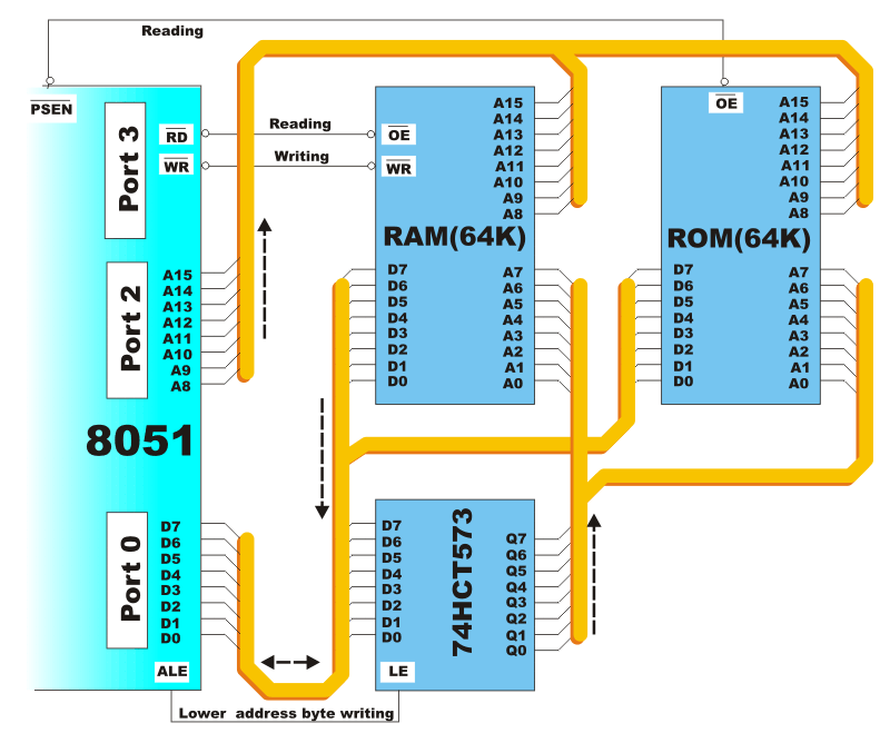
From the users’ perspective, everything functions quite simple if properly connected because the most operations are performed by the microcontroller itself. The 8052 microcontroller has two separate reading signals RD#(P3.7) and PSEN#. The first one is activated byte from external data memory (RAM) should be read, while another one is activated to read byte from external program memory (ROM). These both signals are active at logical zero (0) level. A typical example of such memory extension using special chips for RAM and ROM is shown on the previous picture. It is called Hardward architecture.
Even though the additional memory is rarely used with the latest versions of the microcontrollers, it will be described here in short what happens when memory chips are connected according to the previous scheme. It is important to know that the whole process is performed automatically, i.e. with no intervention in the program.
- When the program during execution encounters the instruction which resides in external memory (ROM), the microcontroller will activate its control output ALE and set the first 8 bits of address (A0-A7) on P0. In this way, IC circuit 74HCT573 which “lets in” the first 8 bits to memory address pins is activated.
- A signal on the pin ALE closes the IC circuit 74HCT573 and immediately afterwards 8 higher bits of address (A8-A15) appear on the port. In this way, a desired location in additional program memory is completely addressed. The only thing left over is to read its content.
- Pins on P0 are configured as inputs, the pin PSEN is activated and the microcon troller reads content from memory chip. The same connections are used both for data and lower address byte.
Similar occurs when it is a needed to read some location from external Data Memory. Now, addressing is performed in the same way, while reading or writing is performed via signals which appear on the control outputs RD or WR.
Addressing
While operating, processor processes data according to the program instructions. Each instruction consists of two parts. One part describes what should be done and another part indicates what to use to do it. This later part can be data (binary number) or address where the data is stored. All 8052 microcontrollers use two ways of addressing depending on which part of memory should be accessed:
Direct Addressing
On direct addressing, a value is obtained from a memory location while the address of that location is specified in instruction. Only after that, the instruction can process data (how depends on the type of instruction: addition, subtraction, copy…). Obviously, a number being changed during operating a variable can reside at that specified address. For example:
Since the address is only one byte in size ( the greatest number is 255), this is how only the first 255 locations in RAM can be accessed in this case the first half of the basic RAM is intended to be used freely, while another half is reserved for the SFRs.
Indirect Addressing
On indirect addressing, a register which contains address of another register is specified in the instruction. A value used in operating process resides in that another register. For example:
Only RAM locations available for use are accessed by indirect addressing (never in the SFRs). For all latest versions of the microcontrollers with additional memory block (those 128 locations in Data Memory), this is the only way of accessing them. Simply, when during operating, the instruction including “@” sign is encountered and if the specified address is higher than 128 (7F hex.), the processor knows that indirect addressing is used and jumps over memory space reserved for the SFRs.
On indirect addressing, the registers R0, R1 or Stack Pointer are used for specifying 8-bit addresses. Since only 8 bits are available, it is possible to access only registers of internal RAM in this way (128 locations in former or 256 locations in latest versions of the microcontrollers). If memory extension in form of additional memory chip is used then the 16-bit DPTR Register (consisting of the registers DPTRL and DPTRH) is used for specifying addresses. In this way it is possible to access any location in the range of 64K.
SFRs (Special Function Registers)
SFRs are a kind of control table used for running and monitoring microcontroller’s operating. Each of these registers, even each bit they include, has its name, address in the scope of RAM and clearly defined purpose ( for example: timer control, interrupt, serial connection etc.). Even though there are 128 free memory locations intended for their storage, the basic core, shared by all types of 8052 controllers, has only 21 such registers. Rest of locations are intensionally left free in order to enable the producers to further improved models keeping at the same time compatibility with the previous versions. It also enables the use of programs written a long time ago for the microcontrollers which are out of production now.
A Register (Accumulator)

This is a general-purpose register which serves for storing intermediate results during operating. A number (an operand) should be added to the accumulator prior to execute an instruction upon it. Once an arithmetical operation is preformed by the ALU, the result is placed into the accumulator. If a data should be transferred from one register to another, it must go through accumulator. For such universal purpose, this is the most commonly used register that none microcontroller can be imagined without (more than a half 8052 microcontroller’s instructions used use the accumulator in some way).
B Register
B register is used during multiply and divide operations which can be performed only upon numbers stored in the A and B registers. All other instructions in the program can use this register as a spare accumulator (A).

During programming, each of registers is called by name so that their exact address is not so important for the user. During compiling into machine code (series of hexadecimal numbers recognized as instructions by the microcontroller), PC will automatically, instead of registers’ name, write necessary addresses into the microcontroller.
R Registers (R0-R7)

This is a common name for the total 8 general purpose registers (R0, R1, R2 …R7). Even they are not true SFRs, they deserve to be discussed here because of their purpose. The bank is active when the R registers it includes are in use. Similar to the accumulator, they are used for temporary storing variables and intermediate results. Which of the banks will be active depends on two bits included in the PSW Register. These registers are stored in four banks in the scope of RAM.
Description:
The AT89S52 is a low-voltage, high-performance CMOS 8-bit microcomputer with 4K bytes of Flash programmable memory. The device is manufactured using Atmel’s high-density nonvolatile memory technology and is compatible with the industry-standard MCS-51 instruction set. By combining a versatile 8-bit CPU with Flash on a monolithic chip, the Atmel AT89S52 is a powerful microcomputer, which provides a highly flexible and cost-effective solution to many embedded control applications.
In addition, the AT89S52 is designed with static logic for operation down to zero frequency and supports two software selectable power saving modes. The Idle Mode stops the CPU while allowing the RAM, timer/counters, serial port and interrupt system to continue functioning. The power-down mode saves the RAM contents but freezes the oscillator disabling all other chip functions until the next hardware reset.
Machine cycle for the 8052
The CPU takes a certain number of clock cycles to execute an instruction. In the 8052 family, these clock cycles are referred to as machine cycles. The length of the machine cycle depends on the frequency of the crystal oscillator. The crystal oscillator, along with on-chip circuitry, provides the clock source for the 8052 CPU.
The frequency can vary from 4 MHz to 30 MHz, depending upon the chip rating and manufacturer. But the exact frequency of 11.0592 MHz crystal oscillator is used to make the 8052 based system compatible with the serial port of the IBM PC.
In the original version of 8052, one machine cycle lasts 12 oscillator periods. Therefore, to calculate the machine cycle for the 8052, the calculation is made as 1/12 of the crystal frequency and its inverse is taken.
[…] 8051/8052 – MEVIHUB A webpage with a lot of infromation on the 8052 processor. […]